Application and Definition of Thermal Resistances on Datasheet
Abstract
Thermal issue has been a crucial topic for a long time since high power density and low cost requirements became popular. As a power engineer, the assessment of maximum allowable power dissipation of every component in the system is one of the most important topics when developing a brand new product with good reliability. Generally, each component has a specific thermal characteristics table, which can be found in the datasheet. There are many thermal resistance listed in the table, including θJA, θJB, θJC…etc. Most of these values are defined under the specific JEDEC standards. The JEDEC standards provide the common criteria for measuring the thermal resistances of an IC package, which can be used by the power engineer to compare the thermal (material) properties of different devices. However, thermal resistances based on JEDEC rules can’t be directly applied to actual applications because of different layout arrangements (number of layout layers, PCB thickness, number of thermal Vias and power traces routing...etc.). Many power engineers are looking for better dependable thermal resistances for estimating the temperature of each component in their real power system. Hence, the alternative thermal parameters named psi-(Ψ) are given on the datasheet. Unlike traditional thermal resistances (θJA, θJB, θJC…etc.), these psi- thermal parameters (ΨJB, ΨJC…etc.) are measured on an evaluation board (EVB) which is very similar to the actual application PCB layout. Therefore, power engineer can use these parameters to calculate the junction temperature once they know the power dissipation of the chip. It can greatly reduce the effort on dealing with thermal issues in a quick way.
In this application note, the definition and applications of thermal resistances are addressed. Thermal resistances according to both JEDEC standard and real PCB conditions are introduced. Moreover, a simple example for describing the difference between these two parameters is given in the last section.
1. Thermal Resistances Defined by JEDEC Standards
In this section, the definition and measurement process of thermal resistances (θJA, θJCx and θJB) are introduced separately. Based on different package types, there are many JEDEC PCB standards. The standards are summarized at the end of this section.
1.1
θJA Thermal Resistances
The thermal resistance θJA (Theta-JA) is the chip junction-to-ambient air thermal resistance measured in the convection environments described in JESD51-2. The value can be used to compare the thermal performance of different packages if all the test conditions listed in Table 1 are similar. The following formula can be used to define the value of θJA :
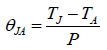
Where P is the “TOTAL” power (heat) dissipated in the chip. TJ is the junction temperature after thermal balance. TA is the ambient temperature. The unit of θJA is in oC/W.
The θJA value is sometimes used to estimate the junction temperature with combination of system ambient temperature in a specific application. However, these estimations are not accurate due to the JEDEC standardized test condition (EVB layout rules) won’t match the user’s application condition.
Following is the measurement process for θJA. The power (heat) can flow through PCB and case top, although most of heat transfers from junction to board in this condition. The contacted board follows the layout rules as defined in JEDEC 51 standards.
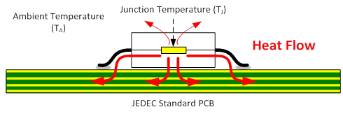
Figure 1. θJA Measurement Process
1.2
θJCx Thermal Resistances
The conduction thermal resistance θJCx (Theta-JCx) is measured with nearly all of the component power dissipation flowing through either the top or the bottom of the package. The “x” indicates the case surface where TCase is measured and through which all the heat is forced to flow during the θJCx measurement, “top” for the top surface or “bot” for the bottom surface. The values may be useful for comparing packages but the test conditions don’t generally match the user’s application. An exception is an application where nearly all of the component heat is flowing through the top of the package to a heat sink (i.e. via a metal mounting tab). θJC(Top) is representative of this application. The following formula can be used to define the value of θJCx :
Where P is the “PART” of the chip power (heat) that flows from the junction to the “x” case surface. Ideally, during θJCx measurement, close to 100% of the power flows from the junction to the “x” case surface. TJ is the junction temperature after thermal balance. The unit of θJCx is in oC/W.
Figures 2 and 3 show the measurement processes for θJC(Top) and θJC(Bottom) respectively. The power (heat) flows in these two cases are opposite. For example, the power can only flow through junction to case top in the measurement process of θJC(Top); on the other hand, the power can only flow through junction to case bottom in the measurement process of θJC(Bottom).
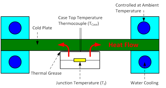
Figure 2. θJC(Top) Measurement Process
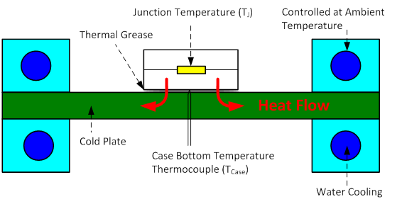
Figure 3. θJC(Bottom) Measurement Process
1.3
θJB Thermal Resistances
θJB is the junction-to-board thermal resistance where TBoard is the temperature measured on or near the component lead, using a 2s2p board, as described in JESD51-8. For a leaded package, the thermocouple is attached to the foot of a lead. For an area array surface mount package, the thermocouple is attached to a board trace within 1mm of the package body. The following formula can be used to define the value of θJB :
Where P is the “PART” of the chip power (heat) that flows from the junction to the board. Ideally, approximately to 100% of the power flows from the junction to the board during θJB measurement using the test fixture specified in JESD51-8. TJ is the junction temperature after thermal balance. The unit of θJB is in oC/W.
To measure θJB, convection from the top of the package is blocked and a cold plate is attached to the board’s far side opposite the package location. See Figure 4 as below. In the moment, most of heats are transferred via bottom board.
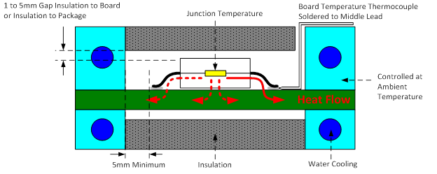
Figure 4. Illustration of the process for measuring θJB
1.4
Summary of JEDEC PCB Standards
According to package type, there are six different PCB standards. JESD51-3 and JESD51-7 apply to leaded surface mount (SMT) packages like flip-chip and QFN packages, and define the 1s (one signal layer) and 2s2p (two signal layers and two power layers) test boards respectively. JESD51-5 extends the test boards to packages with direct thermal attach mechanisms like deep down-set exposed pad packages and thermally tabbed packages. Generally, this applies to the SMT boards defined in JESD51-3 and JESD51-7. JESD51-9 defines test boards for area array SMT packages like ball grid array (BGA) packages. Both 1s and 2s2p test boards are included, as well as the requirements for dealing with thermal balls and vias. JESD51-10 and JESD51-11 define test boards for through-hole leaded packages like pin grid array packages (PGAs). JESD51-10 covers perimeter leaded packages and JESD51-11 covers area array leaded packages. Both 1s and 2s2p test boards are included in both standards. Besides, JESD51-2A addresses the environmental conditions for different packages thermal measurement under nature convection.
Table 1. JEDEC PCB Standards for Different Packages
|
Package Type
|
JEDEC-standard
|
Topic
|
|
All
|
JESD51-2A
|
Integrated Circuits Thermal Test Method Environmental Conditions - Natural Convection (Still Air)
|
|
Leaded Surface Mount Packages
|
JESD51-3
|
Low Effective Thermal Conductivity Test Board for Leaded Surface Mount Packages Low Effective Thermal Conductivity Test Board for Leaded Surface Mount Packages
|
|
Leaded Surface Mount Components
|
JESD51-7
|
High Effective Thermal Conductivity Test Board for Leaded Surface Mount Packages
|
|
Packages with TP (thermal pad)
|
JESD51-5
|
Extension of Thermal Test Board Standards for Packages with Direct Thermal Attachment Mechanisms
|
|
Area Array Surface Mount Package
|
JESD51-9
|
Test Boards for Area Array Surface Mount Package Thermal Measurements
|
|
Through-hole mount perimeter leaded packages
|
JESD51-10
|
Test Boards for Through-Hole Perimeter Leaded Package Thermal Measurements
|
|
Through-Hole Area Array Leaded Package
|
JESD51-11
|
Test Boards for Through-Hole Area Array Leaded Package Thermal Measurements
|
2. Thermal Characterization Parameters Defined by EVB Standard
Referring to JESD51-2A[1] for IC thermal test method environmental conditions, the thermal characterization parameters ΨJT (Psi-JT) and ΨJB (Psi-JB) are measured by IC manufactures in the same environments as θJA, as listed in Table 1. Literally, these characterization parameters are very close to the results measured on actual EVBs. However, for better approach to real condition, the results on EVBs are suggested to replace the values on JEDEC’s high conduction boards. Afterwards, users can apply the Ψ (Psi) equations to estimate the component junction temperature in their application by measuring a component temperature in the application environment and using the appropriate Ψ thermal characterization parameter.
2.1
ΨJT Thermal Characterization
Parameters
ΨJT is the junction-to-top thermal characterization parameter where TTop is the temperature at the top center of the package.

Where P is the “TOTAL” power (heat) dissipated in the chip. As shown in the Figure 5, the power may leave the chip through any thermal path, not just the top of the package. A thermal couple is attached to the top of case center to sense the case temperature. The unit of ΨJT is in oC/W. In practice, the ΨJT value will be much smaller than the θJC(Top) value since the actual heat flow from junction to case top is much less compared to the θJC(Top) measurement condition.
Figure 5. ΨJT Measurement Process
2.2
ΨJB Thermal Characterization
Parameters
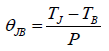
ΨJB is the junction-to-board thermal characterization parameter where TBoard is the temperature measured on or near the component lead. For a leaded package, the thermocouple is attached to the foot of a lead. For an area array surface mount package, the thermocouple is attached to a board trace within 1mm of the package body.

Where P is the “TOTAL” power (heat) dissipated in the chip. As shown in Figure 6, the power may leave the chip through any thermal path, not just the board. A thermal couple is attached to the foot of a lead to sense the board temperature. The unit of ΨJB is in oC/W.
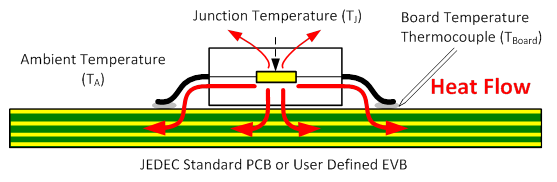
Figure 6. ΨJB Measurement Process of Leaded Package
2.2.1 Considerations for Board Temperature Measurement
According to different types of package or footprints, the measuring position of board temperature (TBoard) should be considered. There are rules summarized as below for reference:
a. Area array package (CSP, QFN) : < 1mm from the package edge (close to ground pin).
b. Leaded package (SOP, TSOT) : < 1mm from the ground pin edge.
c. Choose Rule : Left to Right, more ground pins to less ground pins, clockwise.
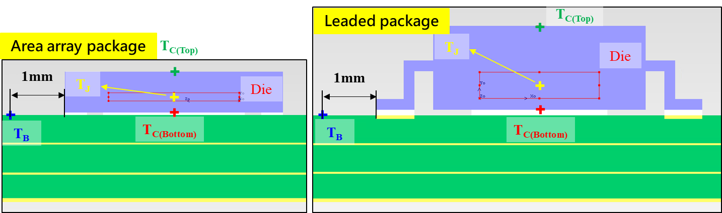
Figure 7. Selection of Board Temperature Measurement for different Package Type
3. Decoupling of Thermal Resistance Network
There are three methods for heat transfer : conduction, convection and radiation. When the temperature difference is generated, the heat will start to flow from high temperature to low temperature. While most of heat will select the medium with smallest thermal resistance, PCB conduction via solder to copper provides the route. An example of thermal resistance network for a chip mounted on PCB is shown in Figure 8.
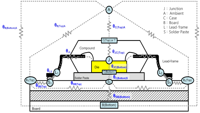
Figure 8. An Example of Thermal Resistance Network
In Figure 8, there are many routes for heat to dissipate in a thermal system. Each route demonstrates an equivalent thermal resistance. In this diagram, they are named with θxy, where xy means the thermal dissipating route from node to node, like junction(J) to case(C), case(C) to ambient(A), solder paste(S) to board(B) etc. Ideally, the θ should be the thermal resistance for physical meaning which related to thermal characteristics of material. However, it’s hard to calculate a specific thermal resistance within a complicated thermal system. Frankly, it is a lumped sum of variety thermal parameters. A simplified thermal resistance network is shown in Figure 9. The symmetric rule of Ohm’s law and thermal resistances are adopted for calculation.
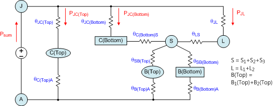
Figure 9. A Simplified Thermal Resistance Network
In the simplified thermal resistance network as shown in Figure 9, there are three synthesized nodes (S, L, B(Top)), where S is an integration of multiple nodes (S1, S2 and S3) standing for a solder paste node, L is an integration of multiple nodes (L1 and L2) standing for a lead-frame node, and B(Top) is an integration of multiple nodes (B1(Top) and B2(Top)) standing for a board node. The Psum is the total heat dissipated from chip’s die, it acts like a current flowing out of die to everywhere in the overall system. The Psum can flow to three routes (junction to case top, junction to case bottom, junction to lead-frame) during heat dissipation. Hence, the Psum distributes to each route depending on the thermal resistance value. According to the definition described in section1 and section2, the thermal resistance (θJC(Top)) defined by JEDEC and thermal characteristic parameter (ΨJC(Top)) defined by EVB can be calculated as below :
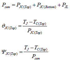
And the junction temperature can be calculated as below :
TJ = TC + ΨJC(Top) × Psum = TC + θJC(Top) × PJC(Top)
It should be noticed that the θJC(Top) should be much larger than ΨJC(Top). Actually, ΨJC(Top) is an equivalent thermal characteristic parameter from junction to case top for a given system instead of real thermal resistance based on material properties. However, ΨJC(Top) is easier to use for temperature estimation in real condition because PJC(Top) is hard to calculate in real cases.
4. Example of Using Thermal Parameters to Estimate Junction Temperature
For a given application, power engineers can calculate the power dissipation of each component in the system. Generally, each component has a maximum allowable operating temperature for reliability considerations. As depicted above, the thermal resistances (θJA, θJCx and θJB) are measured with the conditions of the specific power (heat) transferring direction or a fixed board layout. In real conditions, the power may leave the chip through any thermal path and the layout may not be like the JEDEC PCB, so the estimated junction temperature based on θJA, θJCx and θJB can’t be accurate. Due to the fact that the thermal path is not fixed, ΨJT or ΨJB values may be used with package top or board temperature measurements respectively to provide good junction temperature estimates. In the situation where the component power dissipation is not precisely known, the use of ΨJT may provide a more accurate TJ estimate. This is because the plastic top surface temperature of the component is generally closer to the junction temperature than the board temperature. Therefore, ΨJT is smaller than ΨJB and there is less absolute temperature prediction error.
An application example is described as below :
The RT6253A is a 3A synchronized step-down Buck converter. It is available in TSOT-23-6(FC) package. Since power MOSFETs are embedded inside the chip, thermal estimation is crucial to confirm the acceptable output power rating in case of overheating. The most important thing is keeping the die temperature under the recommended operating condition, which is normally 125°C. Generally, there are many thermal parameters listed in the product’s datasheet as in Table 2. Some parameters are measured based on JEDEC standards, like θJA, θJC(Top) and θJC(Bottom). However, these can’t be directly applied to calculate the junction temperature if ambient temperature or case top temperature or case bottom temperature are known. Because the board conditions are quite different between EVB and JEDEC standard board, and the heat flow of θJC(Top) and θJC(Bottom) measurements are regarded in singular direction, the calculated junction temperature may be far away from the real value. On the other hand, some parameters are measured under the customized EVB, like θJA(EVB), ΨJC(Top) and ΨJB. By measuring the ambient temperature or case top temperature or board temperature and using these parameters, the operating junction temperature can be predicted more accurately.
For a given example application condition, VIN = 12V, VOUT = 1V, IOUT = 3A, TA = 25°C, the thermal measurement result by Fluke Ti450 is as shown in Figure 13. In this case, the maximum top case temperature of IC is 67.4°C and the board temperature at GND pin is 51.6°C. The measuring location of the board temperature is shown in Figure 12. There is a quick method to estimate the power dissipation of chip from thermal parameters as shown in Table 2. Due to ΨCA(Top) is equal to (θJA(EVB) - ΨJC(Top)), the power dissipation can be calculated from DTCA/ΨCA(Top), where both ΨJC(Top) and θJA(EVB) are measured on the EVB. Therefore, the power dissipation is calculated as (67.4-25)/(61-13.9) = 0.9W. The conversion efficiency of this example is 74.85%, the total converter power loss is 1.014W. Which means the residual power loss on inductor and PCB traces is around 0.114W. After that, the maximum junction temperature of IC can be calculated as TJ = (PD_IC x θJA(EVB)) + TA = (0.9W x 61°C/W) + 25°C = 79.9°C. On the other hand, it can also be calculated by ΨJB parameter, and the maximum junction temperature is TJ = (PD_IC x ΨJB) + TBOARD = (0.9W x 31.53°C/W) + 51.6°C = 79.98°C.
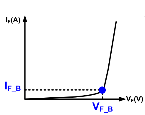
In order to measure the actual junction temperature at PD = 0.9W, we can make use of the thermal characteristic of low-side MOSFET’s body diode in Buck converter IC’s. The experimental setup for diode method is shown in Figure 10. We apply a pulsating current with large duty cycle (DHeat) on the body diode. The high current with large duty cycle applied to this case is IF,Heat = 1.32A to achieve high power dissipation in the IC. The duty cycle low period (1-DHeat) has a low conduction current (for this case, the IF,B = 80mA) which is used to measure the body diode forward voltage and we use this value to estimate the junction temperature. The IF,B is determined according to the VF curve of low-side MOSFET’s body diode as shown in Figure 11(a). A small current at the breaking point is suggested to avoid self-heating and get enough IF tolerance. As a result, the average power dissipation on the chip is 0.9W, which can be calculated by following equation.

Where VF,Heat is the diode forward voltage when conducting with IF,Heat and VF,HighT is the diode forward voltage when conducting with IF,B. The duty cycle of pulsating current is recommended to be 90%.
As shown in Figure 14, because there is some undershoot of IF,B when diode forward current switches from high to low, the voltage at the beginning point of transition is not accurate. Hence, some prediction for V1 point is adopted depending on the linearity of cooling curve after IF is stable at 80mA, V2 point. Then the voltage at V1 point is around 0.633V. Besides, it should be noticed that V2 can’t be directly used for junction temperature estimation since there is some temperature drop after IF,B is stable. Finally, the maximum junction temperature can be calculated by following equation :
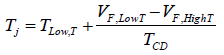
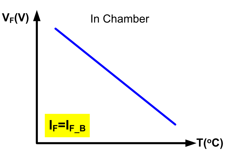
Where TLow,T = 25°C, VF,LowT = 0.732V, VF,HighT = 0.6333V and TCD = 0.0018V/°C. The TJ is 79.83°C. VF,LowT is the diode forward voltage as conducting IF,B at TAmbient = TLow,T. TCD is the temperature coefficient of body diode forward voltage as shown in Figure 11(b) which can be measured in a temperature chamber.
The result shows the junction temperature calculated by θJA(EVB), ΨJC(Top) and ΨJB are match quite well with the result achieved by conducting body diode to estimate the junction temperature.
Figure 10. Diode Method for Junction Temperature Measurement
|
(a)
|
(b)
|
Figure 11. MOSFET Body Diode Characteristic Curves
On the other hand, if we would have used θJC(Top) or θJC(Bottom) for calculating the junction temperature, it would result in (0.9W x 88.7°C/W) + 25°C = 104.83°C, which is much higher than real value of 79.83°C. In principle neither θJC(Top) or θJC(Bottom) are suitable to predict the junction temperature because the actual heat flow does not follow a unique direction.
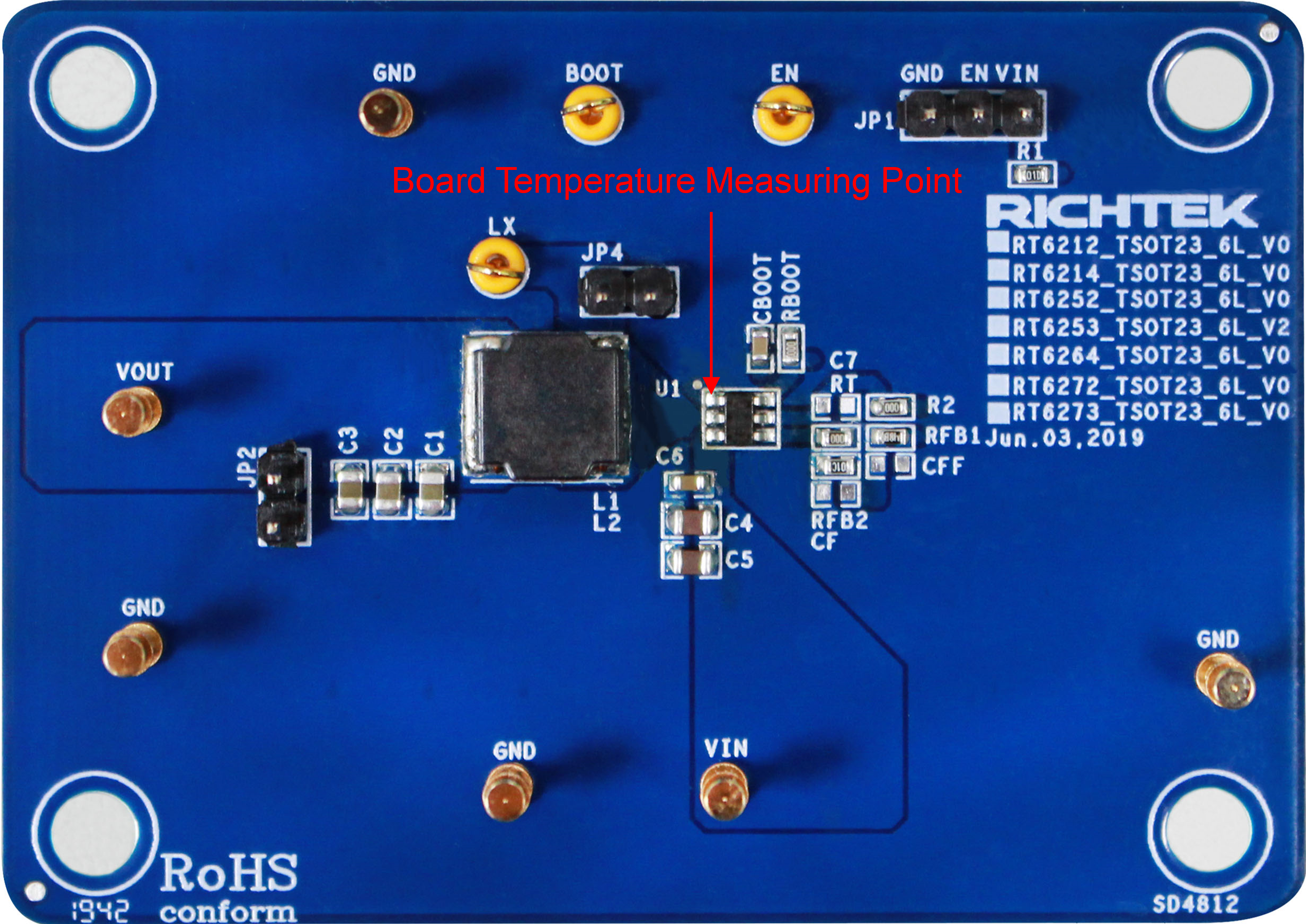
Figure 12. Measuring Point of Board Temperature on RT6253A EVB
Table 2. Thermal Parameters of RT6253A in TSOT-23-6(FC) Package
|
Thermal Parameter
|
TSOT-23-6(FC)
|
Unit
|
|
θJA
|
Junction-to-ambient thermal resistance
(JEDEC standard)
|
88.7
|
°C/W
|
|
θJC(Top)
|
Junction-to-case (top) thermal resistance
|
76.9
|
|
θJC(Bottom)
|
Junction-to-case (bottom) thermal resistance
|
6
|
|
θJA(EVB)
|
Junction-to-ambient thermal resistance
(specific EVB)
|
61
|
|
ΨJC(Top)
|
Junction-to-top characterization parameter
|
13.9
|
|
ΨJB
|
Junction-to-board characterization parameter
|
31.53
|
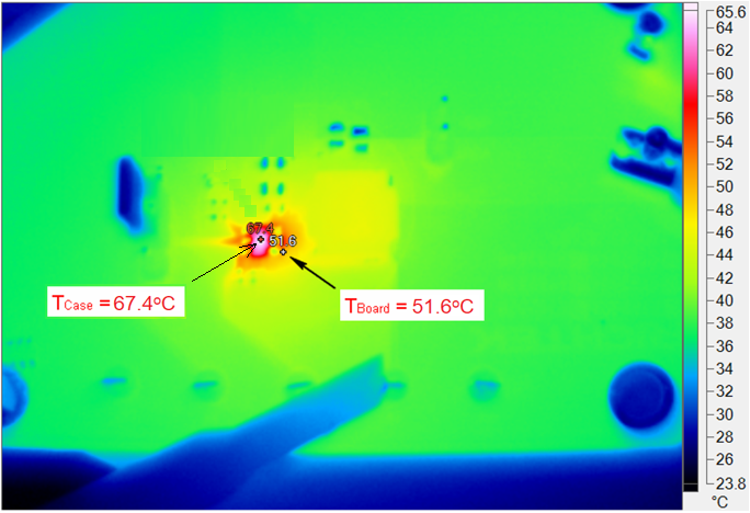
Figure 13. Measurement of Thermal Image by Fluke Ti450
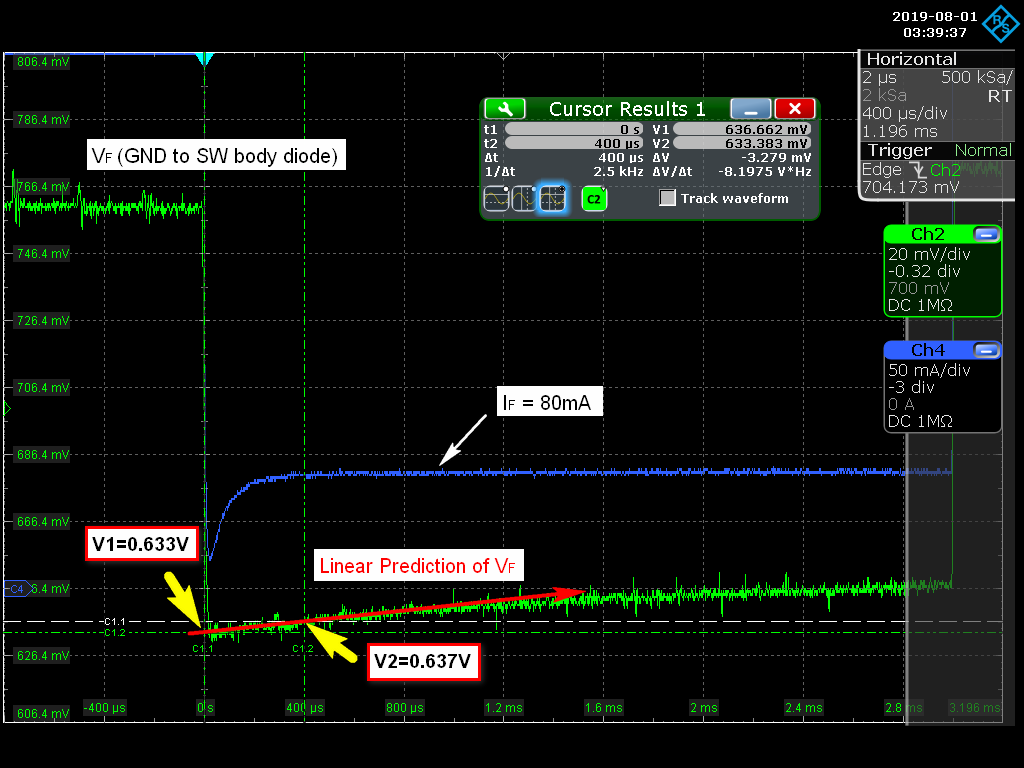
Figure 14. Measurement of Junction Temperature by Diode Method
5. Conclusions
In this application note, the differences between definitions of thermal resistances of θJA, θJB, θJC based on JEDEC standard and psi- thermal parameters of ΨJB, ΨJC based on customized EVB and test condition are addressed. The direction of heat flows very different for the θJB, θJC and ΨJB, ΨJC. In practical conditions, the heat flow depends on the thermal conductivity of material and the heat may leave the chip through multiple thermal paths instead of only one path. Literally, thermal resistances of θJA, θJB, θJC can be applied to compare the thermal conductivity of different packages from different IC suppliers under a standardized environment. On the other hand, the ΨJB, ΨJC thermal parameters are very useful to quickly predict the junction temperature in the actual application operation. An actual application example of these parameters has been provided in the report. The result shows that using the psi- thermal parameters to calculate the junction temperature is much more accurate than when using the JEDEC thermal resistance values.
6. Reference
[1] JESD51-2A, Integrated Circuits Thermal Test Method Environmental Conditions - Natural Convection (Still Air)
[2] JESD51-12, Guidelines for Reporting and Using Electronic Package Thermal Information
[3] SPRA953B, Semiconductor and IC Package Thermal Metrics
[4] SBVA025, Using New Thermal Metrics
[5] RT6253A/B Datasheet